
A brief introduction to organic electronics: solar cells and transistors
Article Sidebar
Main Article Content
Abstract
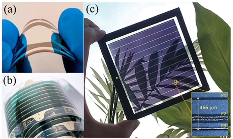
Responsible innovation in developing countries should be part of the university culture. Global innovation processes during the last two decades envision a fast development in humanity with promising applications such as portable, wearable, implantable, and even compatible with biological systems and electronic devices. Innovation as a culture in other research and development centers has achieved successful and exciting advances in different organic electronic devices, such as organic light-emitting diodes, organic photovoltaic systems, organic field-effect transistors, sensors, and memories. Here, an updated review is carried out on the emerging and innovative field of organic electronics. The focus is to provide a clear introduction to the field while highlighting its advantages and disadvantages. Also included are two primary devices considered distinguished in organic electronics: organic solar cells and organic field-effect transistors. For each of the selected devices in this review, the state-of-the-art is addressed, the basic principle of operation is discussed, and examples are highlighted, which sets the point to innovative processes. Finally, a discussion is provided with the perspective for including an innovative field in the research culture of Ecuador.
Downloads
Article Details

This work is licensed under a Creative Commons Attribution 4.0 International License.
Authors who publish in this journal agree to the following terms: Authors retain the copyright and guarantee the journal the right to be the first publication of the work, as well as, licensed under a Creative Commons Attribution License that allows others share the work with an acknowledgment of the authorship of the work and the initial publication in this journal. Authors may separately establish additional agreements for the non-exclusive distribution of the version of the work published in the journal (for example, placing it in an institutional repository or publishing it in a book), with acknowledgment of its initial publication in this journal. Authors are allowed and encouraged to disseminate their work electronically (for example, in institutional repositories or on their own website) before and during the submission process, as it may lead to productive exchanges as well as further citation earliest and oldest of published works.
How to Cite
References
[2] S. Forrest, P. Burrows, and M. Thompson, “The dawn of organic electronics,” IEEE Spectr., vol. 37, no. 8, pp. 29–34, Aug. 2000.
[3] X. Liu et al., “Degradable and dissolvable thin-film materials for the applications of new-generation environmental-friendly electronic devices,” Applied Sciences, vol. 10, no. 4, Feb. 2020.
[4] P. W. M. Blom, “Polymer Electronics: To Be or Not to Be?,” Adv. Mater. Technol., vol. 5, no. 6, May. 2020.
[5] A. V. Marquez, N. McEvoy, and A. Pakdel, “Organic Electrochemical Transistors (OECTs) Toward Flexible and Wearable Bioelectronics,” Molecules, vol. 25, no. 22, Nov. 2020.
[6] S. Kola, J. Sinha, and H. E. Katz, “Organic transistors in the new decade: Toward n-channel, printed, and stabilized devices,” J. Polym. Sci. Part B Polym. Phys., vol. 50, no. 15, pp. 1090–1120, Feb. 2012.
[7] J. J. Gooding, F. Mearns, W. Yang, and J. Liu, “Self-Assembled Monolayers into the 21st Century: Recent Advances and Applications,” Electroanalysis, vol. 15, no. 2, pp. 81–96, Feb. 2003.
[8] A. P. Quist, E. Pavlovic, and S. Oscarsson, “Recent advances in microcontact printing,” Anal. Bioanal. Chem., vol. 381, no. 3, pp. 591–600, Feb. 2005.
[9] K. Fukuda, K. Yu, and T. Someya, “The Future of Flexible Organic Solar Cells,” Adv. Energy Mater., vol. 10, no. 25, May. 2020.
[10] A. R. Murad, A. Iraqi, S. B. Aziz, S. N. Abdullah, and M. A. Brza, “Conducting polymers for optoelectronic devices and organic solar cells: A review,” Polymers, vol. 12, no. 11, pp. 1–47, Nov. 2020.
[11] T. Sekitani and T. Someya, “Stretchable, large-area organic electronics,” Adv. Mater., vol. 22, no. 20, pp. 2228–2246, May. 2010.
[12] F. De-Moya-Anegón, Félix; Herrán-Páez, Estefanía; Bustos-González, Atilio; Corera-Álvarez, Elena; Tibaná-Herrera, Gerardo; Rivadeneyra, “2020 SIR Iber 2020,” Granada, 2020.
[13] S. Lai et al., “Morphology Influence on the Mechanical Stress Response in Bendable Organic Field-Effect Transistors with Solution-Processed Semiconductors,” Adv. Electron. Mater., vol. 4, no. 10, Sep. 2017.
[14] S. Riera-Galindo, F. Leonardi, R. Pfattner, and M. Mas-Torrent, “Organic Semiconductor/Polymer Blend Films for Organic Field-Effect Transistors,” Adv. Mater. Technol., vol. 4, no. 9, Jun. 2019.
[15] E. Pascual-San-José, X. Rodríguez-Martínez, R. Adel-Abdelaleim, M. Stella, E. Martínez-Ferrero, and M. Campoy-Quiles, “Blade coated P3HT:non-fullerene acceptor solar cells: A high-throughput parameter study with a focus on up-scalability,” J. Mater. Chem. A, vol. 7, no. 35, pp. 20369–20382, Aug. 2019.
[16] S. R. Forrest, “The path to ubiquitous and low-cost organic electronic appliances on plastic.,” Nature, vol. 428, no. 6986, pp. 911–918, Apr. 2004.
[17] A. C. Arias, J. D. MacKenzie, I. McCulloch, J. Rivnay, and A. Salleo, “Materials and applications for large area electronics: Solution-based approaches,” Chem. Rev., vol. 110, no. 1, pp. 3–24, Jan. 2010.
[18] S. Allard, M. Forster, B. Souharce, H. Thiem, and U. Scherf, “Organic semiconductors for solution-processable field-effect transistors (OFETs),” Angew. Chemie - Int. Ed., vol. 47, no. 22, pp. 4070–4098, May. 2008.
[19] P. T. Mathew and F. Fang, “Advances in Molecular Electronics: A Brief Review,” Engineering, vol. 4, no. 6, pp. 760–771, Dec. 2018.
[20] F. Hermerschmidt, S. A. Choulis, and E. J. W. List-Kratochvil, “Implementing Inkjet-Printed Transparent Conductive Electrodes in Solution-Processed Organic Electronics,” Adv. Mater. Technol., vol. 4, no. 5, Jan. 2019.
[21] L. Zhou, A. Wanga, S. C. Wu, J. Sun, S. Park, and T. N. Jackson, “All-organic active matrix flexible display,” Appl. Phys. Lett., vol. 88, no. 8, pp. 19–21, Jan. 2006.
[22] C. D. Dimitrakopoulos and P. R. L. Malenfant, “Organic thin film transistors for large area electronics,” Adv. Mater., vol. 14, no. 2, pp. 99–117, Jan. 2002.
[23] H. F. Haneef, A. M. Zeidell, and O. D. Jurchescu, “Charge carrier traps in organic semiconductors: A review on the underlying physics and impact on electronic devices,” J. Mater. Chem. C, vol. 8, no. 3, pp. 759–787, Dec. 2019.
[24] A. C. Arias, F. Endicott, and R. A. Street, “Surface-Induced Self-Encapsulation of Polymer Thin-Film Transistors”, Adv.Mater.,vol. 18,pp. 2900-2904, Oct. 2006.
[25] L. Ji, J. Shi, J. Wei, T. Yu, and W. Huang, “Air-Stable Organic Radicals: New-Generation Materials for Flexible Electronics?,” Adv. Mater., vol. 32, pp. 1908015, Jun. 2020.
[26] M. Suri et al., “Global Photovoltaic Power Potential by Country,” 2020.
[27] T. A. Amollo, G. T. Mola, and V. O. Nyamori, “Organic solar cells: Materials and prospects of graphene for active and interfacial layers,” Crit. Rev. Solid State Mater. Sci., vol. 45, no. 4, pp. 261–288, Jun. 2019.
[28] X. Guan, Z. Xu, and Q. Jia, “Energy-Efficient Buildings Facilitated by Microgrid,” IEEE Trans. Smart Grid, vol. 1, no. 3, pp. 243–252, Nov. 2010.
[29] V. V. Brus, J. Lee, B. R. Luginbuhl, S.-J. Ko, G. C. Bazan, and T.-Q. Nguyen, “Solution-Processed Semitransparent Organic Photovoltaics: From Molecular Design to Device Performance,” Adv. Mater., vol. 31, no. 30, pp. 1900904, May. 2019.
[30] I. Sartori, A. Napolitano, and K. Voss, “Net zero energy buildings: A consistent definition framework,” Energy Build., vol. 48, pp. 220–232, Feb. 2012.
[31] W. Cao et al., “‘Solar tree’: Exploring new form factors of organic solar cells,” Renew. Energy, vol. 72, pp. 134–139, Jul. 2014.
[32] J. Du et al., “Extremely efficient flexible organic solar cells with a graphene transparent anode: Dependence on number of layers and doping of graphene,” Carbon N. Y., vol. 171, pp. 350–358, Sep. 2020.
[33] A. S. Gertsen, M. F. Castro, R. R. Søndergaard, and J. W. Andreasen, “Scalable fabrication of organic solar cells based on non-fullerene acceptors,” Flex. Print. Electron., vol. 5, no. 1, Jan. 2020.
[34] T. S. A. Arias, G. Naranjo-Lopez, D. V. H. Molina, and A. H. F. Gomez, “Work in progress: First steps to university metaevaluation: Research, academy, outreach, innovation, and management,” in IEEE Global Engineering Education Conference, EDUCON, pp. 1854–1857, Apr. 2017.
[35] N. C. Davy et al., “Pairing of near-ultraviolet solar cells with electrochromic windows for smart management of the solar spectrum,” Nat. Energy, vol. 2, no. 8, pp. 1–10, Sep. 2017.
[36] D. J. Milliron, “Ultraviolet photovoltaics: Share the spectrum,” Nat. Energy, vol. 2, no. 8, pp. 1–2, Jun. 2017.
[37] S. Duan, X. Ren, X. Zhang, S. Cheng, and W. Hu, “Screen Printing of Flexible Electronic Devices,” Prog. Chem., vol. 30, no. 4, pp. 429–438, Apr. 2018.
[38] G. Wang, M. A. Adil, J. Zhang, and Z. Wei, “Large-Area Organic Solar Cells: Material Requirements, Modular Designs, and Printing Methods,” Adv. Mater., vol. 31, no. 45, pp. 1805089, Nov. 2019.
[39] S. Yun et al., “New-generation integrated devices based on dye-sensitized and perovskite solar cells,” Energy Environ. Sci., vol. 11, no. 3, pp. 476–526, Jan. 2018.
[40] Q. Bao, S. Braun, C. Wang, X. Liu, and M. Fahlman, “Interfaces of (Ultra)thin Polymer Films in Organic Electronics,” Adv. Mater. Interfaces, vol. 6, no. 1, pp. 1800897, Sep. 2019.
[41] M. Luo et al., “A new non-fullerene acceptor based on the heptacyclic benzotriazole unit for efficient organic solar cells,” J. Energy Chem., vol. 42, pp. 169–173, Jul. 2019.
[42] Y. Diao et al., “Solution coating of large-area organic semiconductor thin films with aligned single-crystalline domains.,” Nat. Mater., vol. 12, no. 7, pp. 665–71, Jun. 2013.
[43] L. Ding, J. Zhao, Y. Huang, W. Tang, S. Chen, and X. Guo, “Flexible-blade Coating of Small Molecule Organic Semiconductor for Low Voltage Organic Field Effect Transistor,” IEEE Electron Device Lett., vol. 1, no. c, pp. 1–1, Mar. 2017.
[44] S. P. Dalawai et al., “A review of spinel-type of ferrite thick film technology: fabrication and application,” J. Mater. Sci. Mater. Electron., vol. 30, no. 8, pp. 7752–7779, Apr. 2019.
[45] L. Hong, H. Yao, Y. Cui, Z. Ge, and J. Hou, “Recent advances in high-efficiency organic solar cells fabricated by eco-compatible solvents at relatively large-area scale,” APL Mater., vol. 8, no. 12, p. 120901, Nov. 2020.
[46] G. Horowitz, R. Hajlaoui, R. Bourguiga, and M. Hajlaoui, “Theory of the organic field-effect transistor,” Synthetic Metals, vol. 101, no. 1-3, pp. 401-404, May 1999.
[47] G. Horowitz, “Organic field-effect transistors,” Adv. Mater., vol. 10, no. 5, pp. 365–377, Jan. 1999.
[48] D. Braga and G. Horowitz, “High-Performance organic field-effect transistors,” Adv. Mater., vol. 21, no. 14–15, pp. 1473–1486, Apr. 2009.
[49] M. Mas-Torrent, D. Den Boer, M. Durkut, P. Hadley, and A. P. H. J. Schenning, “Field effect transistors based on poly(3-hexylthiophene) at different length scales,” Nanotechnology, vol. 15, no. 4, pp. S265–S269, Mar. 2004.
[50] M. Mas-Torrent and C. Rovira, “Novel small molecules for organic field-effect transistors: towards processability and high performance.,” Chem. Soc. Rev., vol. 37, no. 4, pp. 827–838, Feb. 2008.
[51] F. G. Del Pozo et al., “Single crystal-like performance in solution-coated thin-film organic field-effect transistors,” Adv. Funct. Mater., vol. 26, no. 14, pp. 2379–2386, Sep. 2016.
[52] S. Georgakopoulos, F. G. del Pozo, and M. Mas-Torrent, “Flexible organic transistors based on a solution-sheared PVDF insulator,” J. Mater. Chem. C, vol. 3, pp. 12199–12202, Nov. 2015.
[53] S. Riera-Galindo, A. Tamayo, and M. Mas-Torrent, “Role of Polymorphism and Thin-Film Morphology in Organic Semiconductors Processed by Solution Shearing,” ACS Omega, vol. 3, no. 2, pp. 2329–2339, Feb. 2018.
[54] M. Mas-torrent and C. Rovira, “Transistores de efecto de campo basados en moléculas orgánicas (OFETs),” Investig. Química, vol. 105, no. 1, pp. 18–24, Dec. 2008.
[55] M. Mas-Torrent and C. Rovira, “Role of Molecular Order and Solid-State Structure in Organic Field-Effect Transistors,” Chem. Rev., vol. 111, no. 8, pp. 4833–4856, Mar. 2011.
[56] M. Mas-Torrent and C. Rovira, “Tetrathiafulvalene derivatives for organic field effect transistors,” J. Mater. Chem., vol. 16, p. 433, Oct. 2005.
[57] M. Leufgen et al., “High-mobility tetrathiafulvalene organic field-effect transistors from solution processing,” Org. Electron. physics, Mater. Appl., vol. 9, no. 6, pp. 1101–1106, Dec. 2008.
[58] R. Parashkov et al., All-organic field effect transistors, MRS Online Proceedings Library, vol. 769, no. 31, Dec. 2003.
[59] E. Becker et al., “All-organic thin-film transistors patterned by means of selective electropolymerization,” Appl. Phys. Lett., vol. 83, no. 19, pp. 4044–4046, Nov. 2003.
[60] R. A. L. Silva et al., “α-dithiophene-tetrathiafulvalene-a detailed study of an electronic donor and its derivatives,” Eur. J. Inorg. Chem., no. 13, 2013.
[61] F. G. Del Pozo, S. Galindo, R. Pfattner, C. Rovira, and M. Mas-Torrent, “Deposition of composite materials using a wire-bar coater for achieving processability and air-stability in organic field-effect transistors (OFETs),” in Proceedings of SPIE - The International Society for Optical Engineering, vol. 9568, Aug. 2015.
[62] C. C. Chang, C. L. Pai, W. C. Chen, and S. A. Jenekhe, “Spin coating of conjugated polymers for electronic and optoelectronic applications,” Thin Solid Films, vol. 479, no. 1–2, pp. 254–260, May. 2005.
[63] M. Richard et al., “Large-scale patterning of π-conjugated materials by meniscus guided coating methods,” Adv. Colloid Interface Sci., vol. 275, Jan. 2020.
[64] S. Riera-Galindo, F. Leonardi, R. Pfattner, and M. Mas-Torrent, “Organic Semiconductor/Polymer Blend Films for Organic Field-Effect Transistors,” Adv. Mater. Technol., vol. 4, no. 9, pp. 1–20, Jun. 2019.